


Prototype Business
Tianma Japan offers high reliability and quality products that utilizes own LCD manufacturing capability/know-hows, provides various type of film deposition, patterning and glass cutting, and can be a partner who can cooperate in the development of new technologies and new products in material, processing, machine manufacturers and research institutes.
Feature of prototype
| • Integrated process (deposition, patterning, cutting) |
| • Various metal materials, inorganic insulating film materials, and organic insulating film materials are available |
| • Support small-quantity level trial production to mass production. |
| • Support design such as CAD works. |
| • Support the production of products not only LCD and the contract processing of prototypes using LCD manufacturing technology, equipment, and know-how. |
| • Thick Cu wiring processing with Cu plating is available. |
| • Measurement such as thickness of layer for samples is an option. Please let us know. |
| • Mounting IC, assembling FPC to glass are an option. Please let us know. |
| • Reliability test is an option. Please let us know. |
 |
Available process
■Substrate processing *Process based on 550x660mm and thickness of glass:0.5mm or 0.7mm.
|
Process |
Equipment |
Remarks |
|
|
Cleaning |
UV/Chemical/Highpressure/Ultrasonic/Pure water |
|
|
|
Deposition |
Metal |
Sputter |
AlNd, MoNb, ITO, Cr, Cu,Ti etc |
|
Insulator (inorganic) |
P-CVD * |
SiNx, SiOx, etc. |
|
|
Insulator (organic) |
Spin coater |
Acrylic resin, Polyimide resin |
|
|
Semiconductor |
P-CVD, Sputter |
a-Si, InGaZnO₄ |
|
|
Patterning Photolithography |
Coating resist |
Spin coater |
|
|
Exposure
*Tianma Japan can support design |
Aligner |
Processing ability≥4μm |
|
|
Stepper |
Processing ability≥4μm |
||
|
Development |
Development |
Developer solution: TMAH 2.38% or 0.4% |
|
|
Etching |
Dry etching |
SiOx, SiNx, Cr |
|
|
Wet etching |
AlNd, MoNb, ITO, Cu, Ag |
||
|
Stripping |
Amine based treatment |
||
|
High temperature annealing(bake) |
Hot air circulation |
O2 concentration can be adjusted by N2 |
|
*Please refer to the following table for the thickness of each material.
*Pegarding P-CVD, film formation is possible even on small sized substrates and silicon wafers.
| CVD equipment slot | CVD equipment | ITO sputter |
 |
 |
 |
| Photolithography equipment slot | Stepper | Dry etching equipment |
 |
 |
 |
Table1:Deposition material, Thickness, Line width, Resistance
Below is available type of material, thickness.
|
|
Type |
Thickness |
Minimum line width / Spacing(μm) |
Ratio value |
Remark |
|
Wiring/ |
AL alloy |
30~500 |
4/5 |
5 |
With Mo Alloy lamination |
|
Mo alloy |
30~300 |
4/4.5 |
16 |
||
|
ITO (Transparent conductive) |
40~200 |
4/5 |
165~800 |
||
|
Cr |
30~50 |
4/4 |
20 |
||
|
Cu |
30~200 |
4/9 |
2 |
||
|
Ti |
25~100 |
- |
80 |
Ti layer patterning is not available. |
Thickness, line width and spacing is just guideline.
Measurement such as thickness of layer for samples is an option. Please let us know.
Table2:Material, Thickness, Line width
|
|
Type |
Thickness |
Minimum line width / Spacing(μm) |
Remark |
|
Insulator |
SiNx |
50~1000 |
5 |
Contact hole formation available |
|
SiOx |
50~200 |
5 |
||
|
Acrylic resin |
800~30000 |
10 |
||
|
Polyimide resin |
550~3000 |
10 |
||
|
a-Si |
10~250 |
5 |
|
|
|
InGaZnO₄ |
30~200 |
5 |
Thickness, line width and spacing is just guideline. If you have request, please let us know.
Measurement such as thickness of layer for samples is an option. Please let us know.
■Post-process
|
Available contents |
Equipment |
Remark |
|
Sealing |
Dispensing |
Seal width:0.5~2mm level |
|
ODF |
ODF equipment |
Alignment level:±6μm |
|
Thermosetting Seal material |
Hot air circulation |
|
|
Slimming |
Chemical etching(outsource) |
Up to 0.2t on one side |
|
Cutting |
Regular cutting machine Free form cutting machine |
tolerance:±0.3mm Please ask the cutting size and free form shape. |
|
Polishing edge |
Polishing machine | Size:100mm□~550mm□ |
|
Cleaning |
Pure water cleaning |
*Orientation processing (alignment film printing, rubbing (photoalignment), etc is not available.
■Bonding
|
Available contents |
Equipment |
Remark |
|
Bonding |
Film bonding device machine |
Available size (middle size) Available size (large size) |
|
Sensor & Touch panel bonding |
Includes vacuum bonding UV curing treatment by OCR |
Available size 87x142~325x490mm |
|
OCA bonding |
||
| Touch panel bonding to LCD module |
Includes vacuum bonding UV curing treatment by OCR |
|
|
OCA bonding |
||
|
Adhesive bonding |
| Film bonding device machine | Vacuum bonding equipment |
 |
|
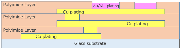
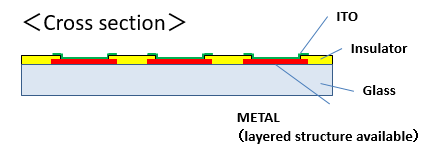
■Plated wiring board processing
The following plated wiring processing is available.
*Processing based on 550x660mm 0.5/0.7t glass substrates is available.
|
Film type |
Available film thickness and line width [μm] |
Remark |
|
Cu plating thickness |
2~12 |
Formed on seed Cu/Ti |
|
Polyimide layer thickness |
6~15 |
|
|
Cu plating: Minimum line width/spacing |
5/5 |
Varies depending on Cu film thickness |
|
Contact Hole Diameter |
>10 |
Varies depending on polyimide film thickness |
|
Au/Ni plating thickness |
standard 0.05/3 |
|
Cross section |
 |
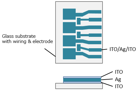
Case of product 1: LCD materials evaluation
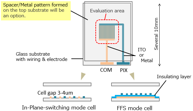 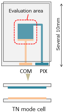 |
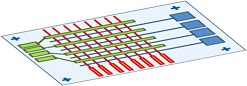
Tianma Japan offers the substrate for evaluation of Liquid Cristal , Polyimide materials.
Case of product 2: OLED materials evaluation
 Offering the substrate for OLED materials. |
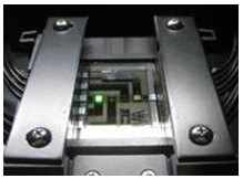 Tianma Japan Sample image |
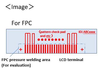
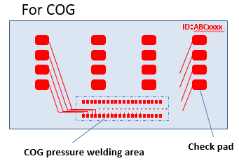
Case of product 3: ACF material evaluation
  |
 |
Tianma Japan supports test samples for evaluation ACF materials.